Obtain news and background information about sealing technology, get in touch with innovative products – subscribe to the free e-mail newsletter.
- Home
-
 Back to
News & Stories
Back to
News & Stories
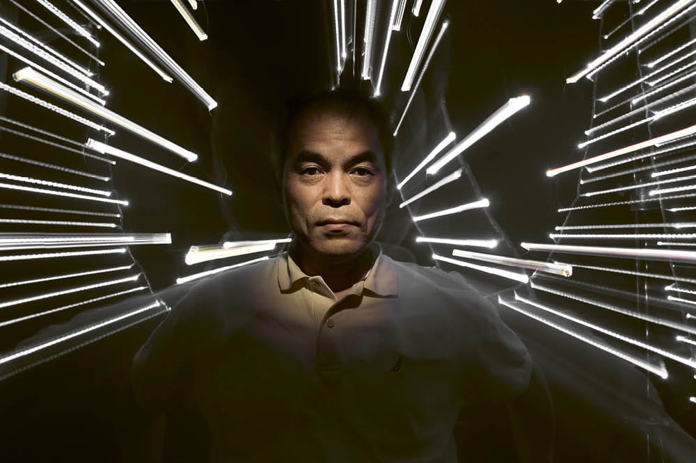
- “Trust Your Own Creativity!”
06.12.2022 | Story
“Trust Your Own Creativity!”
For three decades, blue light-emitting diodes seemed an impossibility. Then, a Japanese engineer made a breakthrough in 1993 by turning to a material that everyone else had written off. An interview with Shuji Nakamura, a Nobel Prize winner in physics, on the limits of research, fires in the lab, and the light that is changing the world.
Dr. Nakamura, your career actually began somewhat unusually.
Dr. Nakamura: You mean because I started out at a chemical company in 1979, even though I was an electrical engineer right out of college?
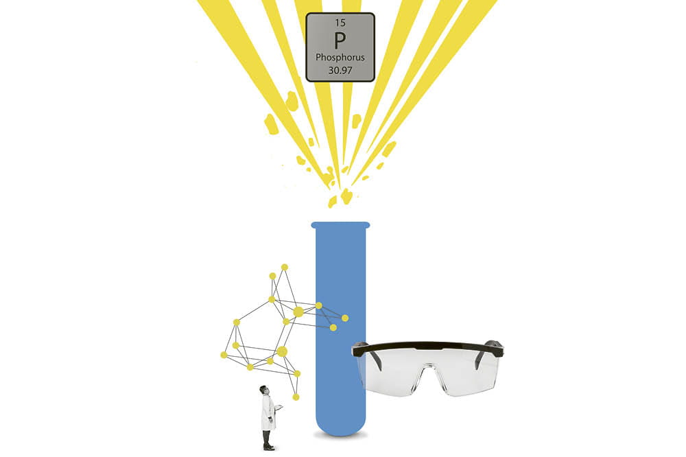
Yes. Nichia produced phosphorus. There was no direct connection to electronics.
The company was looking for new markets. One idea was to use phosphorus to produce gallium phosphide, a semiconductor material for red light diodes. That was my assignment. In any case, I had already worked with compound semiconductors during my studies.
Shuji Nakamura
Born in 1954, he worked for Nichia (then a small company but today one of the world’s largest manufacturers of LEDs) after completing his studies in electrical engineering. He developed the first bright gallium nitride light-emitting diode and was awarded his doctorate from the University of Tokushima in 1994. His other research successes include an indium-gallium nitride LED and a blue laser. In 2001, he sued Nichia, arguing that the company had inadequately remunerated him for his research successes with the equivalent of an approximately 150-euro bonus. The two parties ultimately agreed on 6 million euros, so far the largest bonus ever in Japan. Today, Nakamura is an American citizen. In 2014, along with Isamu Akasaki and Hiroshi Amano, he received the Nobel Prize in physics for his LED research.
Still, you weren’t actually a material developer.
I had to teach myself how to grow crystals from gallium and phosphorus. That required heating the materials to more than 1,000°C (1,832°F). Now just imagine: My office had about 10 square meters (about 108 square feet) of space – and phosphorus is explosive. If you heat it too much and it reacts with oxygen, you get an explosion and flames rising to the ceiling. Burning phosphorus flies in all directions. That occurred about once a month.
Experimenting: For progress one has to ignore everything that seems certain and be creative.
That actually happened?
Yes, at about 5 o’clock in the afternoon, when my coworkers were on the way to the parking lot, the temperature would reach 1,100°C (2,012°F). When the material exploded and I doused the fire with water, there was an impressive amount of smoke. In the beginning, employees would come in and ask me whether everything was all right. I was never actually hurt.
With all due respect, that sounds bizarre from today’s perspective.
Well, the company was out in the country. This would not have been possible in the middle of Tokyo. One problem was that I needed quartz test tubes for the process. The ones that we had were openended, so I had to fuse them myself. The more I mastered all the processes, the fewer explosions there were.
In just three years, Shuji Nakamura succeeded in mass-producing gallium phosphide. But since the company was small, the market’s response was tentative. So its sales team came up with an idea: If you already know the technology for semiconductor materials, why not go ahead and produce red light diodes? Nakamura provided the necessary steps. And he made a decision: He wanted to do more. He wanted to invent blue LEDs.
Your breakthrough leading to blue LEDs began with a bold decision: You selected gallium nitride as the semiconductor material.
The reason was quite simple. I wanted to finally earn my doctorate. In Japan, you have to publish your research results to get it. I thought to myself, hundreds of papers have already been written on zinc selenide. Everyone believed it was the semiconductor material that would deliver the breakthrough. There was hardly anything on gallium nitride. I was able to experiment and do new research on it.
It is hard to escape the personal magnetism of Shuji Nakamura. He is reserved and modest in a refined way, yet approachable and likable at the same time. What he almost dismisses as a coincidence fell in line with a series of advances in material development that he had tackled with determination and creativity – quickly putting himself years ahead of research departments and universities.
If you want to make crystal layers for a lightemitting diode, you need an MOCVD, a very expensive machine that I was not familiar with. Our plan was for me to spend a year at the University of Florida and become acquainted with the technology there. Instead, I had to spend 10 months assembling a machine that had just been delivered.
Research always involves setbacks. If you want to make progress, you have to experiment.
So that wasn’t the plan…
No, but it gave me a very fundamental understanding of the technology. When I started to experiment with gallium nitride, I was able to adapt the machine, rebuilding and re-welding individual parts. Researchers don’t normally do that. They need technicians for this. And technicians have little understanding of materials research.

Blue light-emitting diodes: A Nobel prize winning invention.
It seems as though each apparent setback actually moved you forward in the end.
Research always involves setbacks. If you want to make progress, you have to experiment. I have read a lot on the subject, but you have to stop reading at some point and be creative. You have to ignore everything that seems certain.
Like the fact that all the experts rejected gallium nitride as a semiconductor material?
Well, sometimes the research papers are wrong, too. You can’t develop your own ideas if you are always replicating. I always say: Trust your own creativity. The truth lies in your experiments.
You were a lone wolf. You were practically the entire development department – was it an advantage to be so independent?
Yes. Curiously, other material developers later told me that I was lucky. These were people who worked in departments with a dozen other researchers. But nine out of 10 would say, “Let’s do research on zinc selenide,” and the sole creative voice is outvoted. I could decide on my own. I was the only one in the company who had immersed himself in the subject. Sometimes it is individuals who have to come up with the crazy ideas.
What Nakamura has presented so positively was a complicating factor for a while: On a number of occasions, the management wanted to terminate his research. For a long time, he had a small budget and inadequate equipment, which he improved on his own. He was passed over for raises and did some of his work in defiance of top management.
Are luck and coincidence always factors in inventions?
They at least play a role. People have been doing research on LEDs since the 1970s. There was progress. There were even experiments with gallium nitride. But for a really bright light-emitting diode, you have to improve the electrical conductivity of the semiconductor. You need negatively and positively charged material. For a long time, people thought that positive gallium nitride was an impossibility. The material had other weaknesses as well, but in the end it turned out that some of the weaknesses weren’t important. On the other hand, the potential light yield was huge. The next hurdle was producing indium-gallium nitride with sufficient quality to generate blue light. And everyone considered that to be impossible.
It makes sense for companies to think in terms of products. Scientists can give free rein to their desire to contribute to humanity’s progress.
Today you no longer work for a company – you have been employed at a university since 1999. What difference does that make for development work?
In a company, you rarely have to worry about financing. But it is generally a challenge at universities. We also have high turnover here. Students stay for five years on average. The advantage is that we can be crazier and more creative. At a company, a product has to ultimately emerge.
Does it limit a researcher’s work to be tied to a product or does it also provide focus?
Both. It makes sense for companies to think in terms of products. Scientists can give free rein to their desire to contribute to humanity’s progress. Otherwise, there is the risk that their work could remain theoretical. In the end, it is products that move humanity forward.
What areas are you interested in right now?
Lasers continue to be a multi-layered field. Laser diodes can advance quantum computing and nuclear fusion. Both are exciting areas for the future. In all, there are a great many advances to which laser diodes and lightemitting diodes are contributing. Think about how important LEDs are to sustainability: We are saving huge amounts of energy because they produce more light and less heat.
What would be your advice to future material developers?
The fact that they have to run risks at some point. Once you have mastered the fundamentals, it all comes down to creative execution.
This article originally appeared in ESSENTIAL, Freudenberg Sealing Technologies’ corporate magazine that covers, trends, industries and new ideas.
More news on the subject Technology & Innovation
Technology & Innovation
Solving Today’s Challenges to Power Tomorrow’s Mobility
Freudenberg Sealing Technologies to showcase advanced solutions at the 2025 Battery Show North America

Technology & Innovation
High-Performance Radar Sensors Thanks to Precisely Manufactured Waveguide Antennas
Waveguide antennas with their delicate channel structure are fundamental to the performance of radar sensors. Freudenberg Sealing Technologies is now developing these antennas for its first customer projects.
Technology & Innovation
A High-Pressure Gasket With an Innovative Design for PEM Electrolyzers
High-pressure gaskets keep liquid and gaseous media from escaping electrolyzers. Freudenberg Sealing Technologies has developed a gasket design that is already used in series production.
Technology & Innovation
Electrolysis: Global Market Leader Uses Freudenberg Seals
AEM electrolyzers offer customers the opportunity to produce green hydrogen on their own. The global leader in AEM technology relies on seals from Freudenberg Sealing Technologies.
Technology & Innovation
Simulation on Test Stands
Freudenberg Sealing Technologies not only offers materials expertise. The company also simulates how effective and efficient its products are with the help of its own high-quality test stands.

Technology & Innovation
High Technology in Agriculture
Artificial intelligence, robotics and the Internet of Things are turning agriculture into a high-tech industry. And they are bringing food security to future generations.

Technology & Innovation
Perfect Tire Pressure For Every Terrain
Sealing solutions from Freudenberg Sealing Technologies for central tire inflation systems offer major advantages

Technology & Innovation
Revolutionizing Heavy Duty On Road Mobility
Freudenberg Sealing Technology's Innovative Solution

Technology & Innovation
High Flexibility: “Artificial Intelligence as a Service”
Scalability: With Artificial Intelligence as a Service, AI is always available at the level needed for the current data needs or for the number of inquiries to be processed.

Join Us!
Experience Freudenberg Sealing Technologies, its products and service offerings in text and videos, network with colleagues and stakeholders, and make valuable business contacts.
Connect on LinkedIn! open_in_new